
Author Affiliations
Abstract
1 College of Physics, MIIT Key Laboratory of Aerospace Information Materials and Physics, Key Laboratory for Intelligent Nano Materials and Devices, Nanjing University of Aeronautics and Astronautics, Nanjing 211106, China
2 e-mail: cxkan@nuaa.edu.cn
Low-power, flexible, and integrated photodetectors have attracted increasing attention due to their potential applications of photosensing, astronomy, communications, wearable electronics, etc. Herein, the samples of ZnO microwires having -type (Sb-doped ZnO, ZnO:Sb) and -type (Ga-doped ZnO, ZnO:Ga) conduction properties were synthesized individually. Sequentially, a homojunction vertical structure photodiode involving a single ZnO:Sb microwire crossed with a ZnO:Ga microwire, which can detect ultraviolet light signals, was constructed. When exposed under 360 nm light illumination at , the proposed photodiode reveals pronounced photodetection features, including a largest on/off ratio of , responsivity of 2.3 A/W, specific detectivity of Jones, noise equivalent power of , and superior photoelectron conversion efficiency of . The photodiode also exhibits a fast response/recovery time of 0.48 ms/9.41 ms. Further, we propose a facile and scalable construction scheme to integrate a microwires homojunction component into a flexible, array-type detector, which manifests significant flexibility and electrical stability with insignificant degradation. Moreover, the as-constructed array unit can be integrated into a practical photoimaging system, which demonstrates remarkable high-resolution single-pixel imaging capability. The results represented in this work may supply a workable approach for developing low-dimensional ZnO-based homojunction optoelectronic devices with low-consumption, flexible, and integrated characteristics.
Photonics Research
2024, 12(4): 648

Author Affiliations
Abstract
1 College of Science, MIIT Key Laboratory of Aerospace Information Materials and Physics, Key Laboratory for Intelligent Nano Materials and Devices, Nanjing University of Aeronautics and Astronautics, Nanjing 211106, China
2 e-mail: cxkan@nuaa.edu.cn
has attracted considerable attention due to its wide bandgap, large exciton binding energy, and outstanding electrical and optoelectronic features. Owing to the lack of reliable and reproducible p-type , many challenges on developing -based optoelectronic devices and their practical applications still remain. Herein, single-crystal microwires (MWs) are acquired via the self-catalyzed approach. As a strategic alternative, MW/p-GaN heterojunction was constructed, which exhibited selectable dual-functionalities of light-emitting and photodetection when operated by applying an appropriate voltage. The device illustrated a distinct near-ultraviolet light-emission peaking at and a linewidth . Significantly, the device characteristics, in terms of the main peak positions and linewidth, are nearly invariant as functions of various injection current, suggesting that quantum-confined Stark effect is essentially absent. Meanwhile, the identical MW/p-GaN heterojunction can also achieve photovoltaic-type light detection. The device can steadily feature ultraviolet photodetecting ability, including the ultraviolet/visible rejection ratio () , high photodark current ratio of , fast response speed of 9.2/51 ms, maximum responsivity of 1.5 A/W, and detectivity of Jones under 360 nm light at bias. Therefore, the bifunctional device not only displays distinct near-ultraviolet light emission, but also has the ability of high-sensitive ultraviolet photodetection. The novel design of MW/p-GaN heterojunction bifunctional systems is expected to open doors to practical application of microstructures/nanostructures for large-scale device miniaturization, integration and multifunction in next-generation high-performance photoelectronic devices.
Photonics Research
2021, 9(12): 12002475
Author Affiliations
Abstract
1 College of Science, Nanjing University of Aeronautics and Astronautics, Nanjing 210016, China
2 Key Laboratory for Intelligent Nano Materials and Devices (MOE), Nanjing University of Aeronautics and Astronautics, Nanjing 210016, China
3 e-mail: cxkan@nuaa.edu.cn
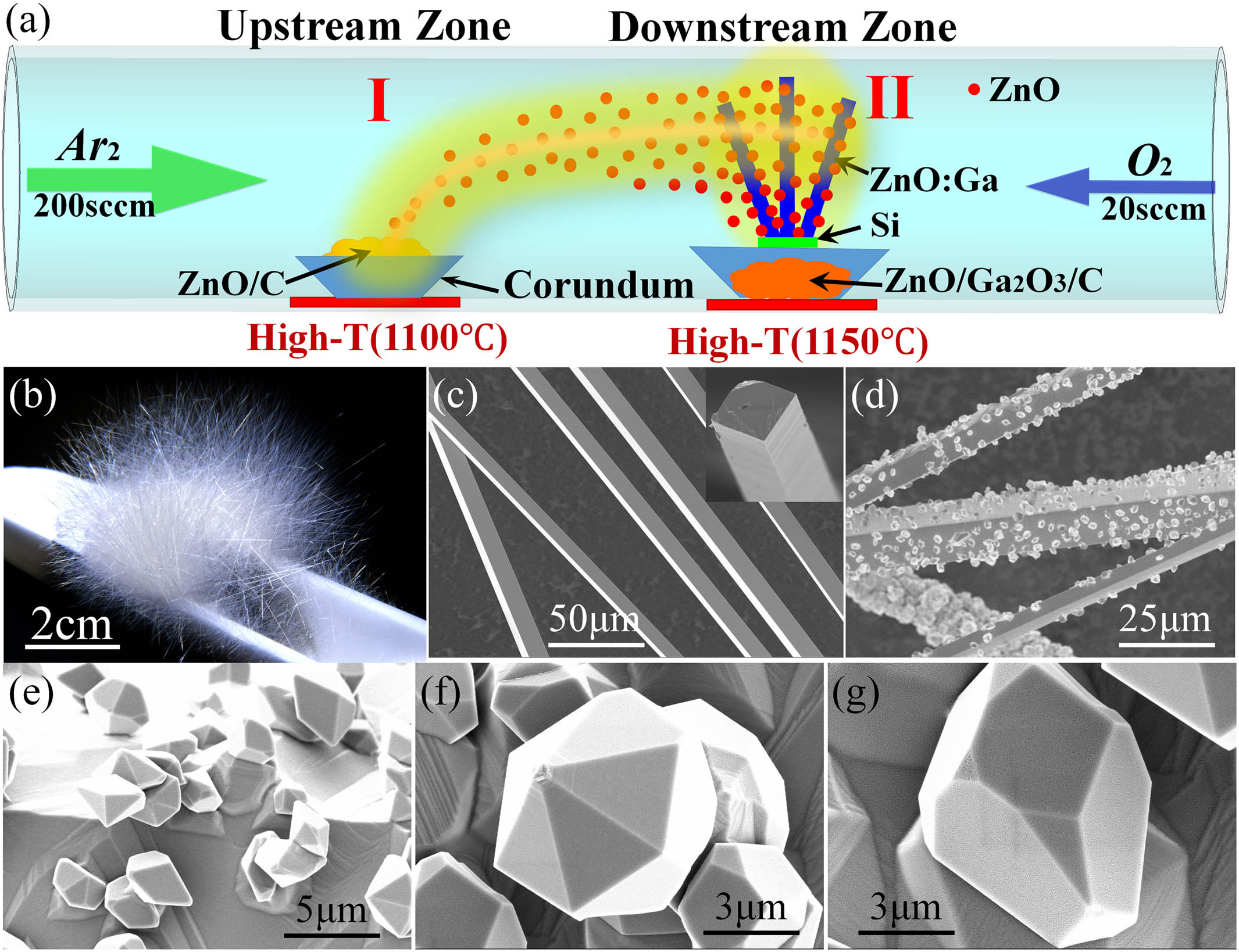
Due to their outstanding surface-to-volume ratio, highly smooth surface, and well-defined crystal boundary, semiconducting micro-/nanocrystals have been used as a pivotal platform to fabricate multifunctional optoelectronic devices, such as superresolution imaging devices, solar concentrators, photodetectors, light-emitting diodes (LEDs), and lasers. In particular, micro-/nanocrystals as key elements can be employed to tailor the fundamental optical and electronic transport properties of integrated hetero-/homostructures. Herein, ZnO microcrystal-decorated pre-synthesized Ga-doped ZnO microwire (ZnO@ZnO:Ga MW) was prepared. The single ZnO@ZnO:Ga MW can be used to construct optically pumped Fabry–Perot (F–P) mode microlasers, with the dominating lasing peaks centered in the violet spectral region. Stabilized exciton-polariton emissions from single ZnO@ZnO:Ga MW-based heterojunction diode can also be realized. The deposited ZnO microcrystals can facilitate the strong coupling of F–P optical modes with excitons, leading to the formation of exciton-polariton features in the ZnO@ZnO:Ga MW. Therefore, the waveguiding lighting behavior and energy-band alignment of ZnO microcrystal-sheathed ZnO:Ga MW radial structures should be extremely attractive for potential applications in semiconducting microstructure-based optoelectronic devices, such as micro-LEDs, laser microcavities, waveguides, and photodetectors.
Photonics Research
2020, 8(2): 02000175
Author Affiliations
Abstract
1 State Key Laboratory of Luminescence and Applications, Changchun Institute of Optics, Fine Mechanics and Physics, Chinese Academy of Sciences, Changchun 130033, China
2 University of Chinese Academy of Sciences, Beijing 100049, China
3 College of Science, Nanjing University of Aeronautics and Astronautics, Nanjing 210016, China
4 School of Physics and Engineering, Zhengzhou University, Zhengzhou 450052, China
5 e-mail: cxshan@zzu.edu.cn
6 e-mail: shendz@ciomp.ac.cn
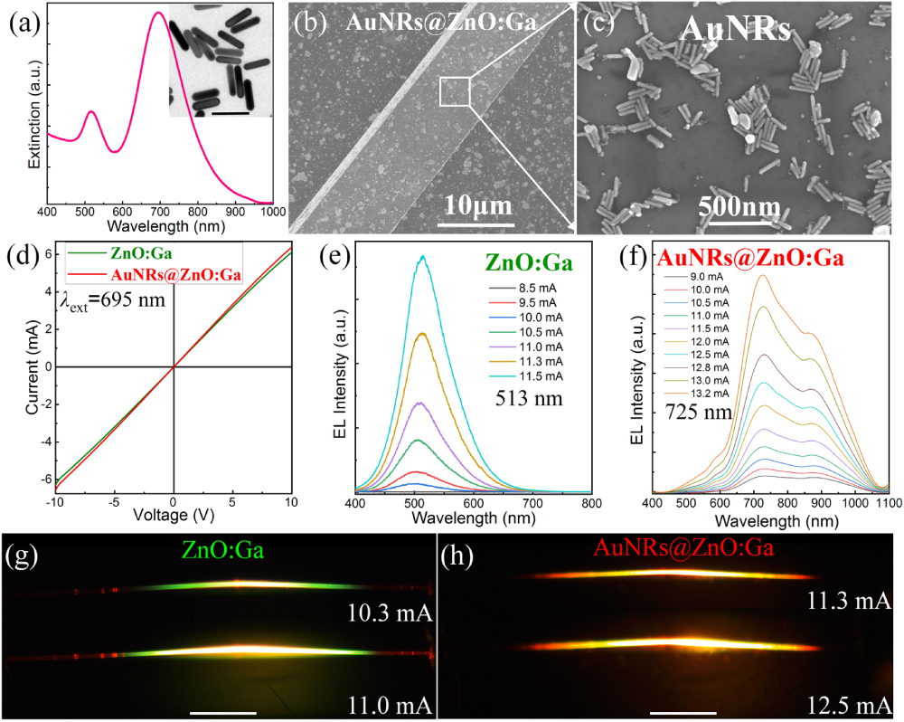
The collective oscillation of electrons located in the conduction band of metal nanostructures being still energized, with the energy up to the bulk plasmon frequency, are called nonequilibrium hot electrons. It can lead to the state-filling effect in the energy band of the neighboring semiconductor. Here, we report on the incandescent-type light source composed of Au nanorods decorated with single Ga-doped ZnO microwire (AuNRs@ZnO:Ga MW). Benefiting from Au nanorods with controlled aspect ratio, wavelength-tunable incandescent-type lighting was achieved, with the dominating emission peaks tuning from visible to near-infrared spectral regions. The intrinsic mechanism was found that tunable nonequilibrium distribution of hot electrons in ZnO:Ga MW, injected from Au nanorods, can be responsible for the tuning emission features. Apart from the modification over the composition, bandgap engineering, doping level, etc., the realization of electrically driving the generation and injection of nonequilibrium hot electrons from single ZnO:Ga MW with Au nanostructure coating may provide a promising platform to construct electronics and optoelectronics devices, such as electric spasers and hot-carrier-induced tunneling diodes.
Photonics Research
2020, 8(1): 01000091

Author Affiliations
Abstract
1 College of Science, Nanjing University of Aeronautics and Astronautics, Nanjing 210016, China
2 Key Laboratory for Intelligent Nano Materials and Devices of the Ministry of Education, Nanjing 210016, China
3 SEU-FEI Nano-Pico Center, Key Laboratory of MEMS of the Ministry of Education, Southeast University, Nanjing 210096, China
4 Southeast University-Monash University Joint Research Institute, Suzhou 215123, China
5 e-mail: cxkan@nuaa.edu.cn
6 e-mail: helongbing@seu.edu.cn
Bio-chemical molecular detection in the nanoscale, based on alloyed nanorods (NRs) with tunable surface plasmon resonance (SPR) properties and high chemical stability, has attracted particular interest. In this work, alloyed Au-Ag NRs with tunable aspect ratios were achieved by annealing Au nanobipyramid-directed Au@Ag core-shell NRs. The core-shell NRs were encapsulated within mesoporous silica outer shells to avoid fusion or aggregation. The structural stability of fully alloyed Au-Ag NRs, including chemical and thermal stability, is remarkably improved compared with that of Au@Ag core-shell NRs. The alloyed NRs would maintain the rod-like structure after being incubated in etchant solution, while Au@Ag core-shell NRs would decay into nanobipyramids. Additionally, fully alloyed NRs present stable morphology under annealing at high temperatures of up to 600°C in air. Benefiting from excellent structural and chemical stabilities, the surface-enhanced Raman scattering effect based on alloyed NRs is stable in harsh environments. Taking advantage of tunable SPR properties (600–1800 nm) and excellent stability, the obtained nanostructures can serve as drug carriers. The perfect photo-thermal effect induced by the particular SPR of alloyed NRs can improve the release efficiency of drugs.
Photonics Research
2019, 7(5): 05000558

Author Affiliations
Abstract
1 College of Science, Nanjing University of Aeronautics and Astronautics, Nanjing 210016, China
2 Department of Mathematics and Physics, Nanjing Institute of Technology, Nanjing 211167, China
Through anisotropic Ag overgrowth on the surface of Au nanobipyramids (AuNBPs), high-purity and sizecontrolled Ag nanorods (Au/AgNRs) are obtained by a simplified purification process. The diameters of the Au/AgNRs are determined by the size of the as-prepared AuNBPs, and the lengths of the Au/AgNRs are tunableusing different amounts of Ag precursor in the growth solution. Surface-enhanced Raman scattering (SERS) studies using Rhodamine-6G (R6G) as a test molecule indicate that the Au/AgNRs have excellent sensing potential. The tunable optical properties and strong electromagnetic effect of the Au/AgNRs, along with their superior SERSsignal enhancement, show that Au/AgNRs are promising for further applications in plasmon sensing and biomolecular detection.of Nanjing Institute of Technology (CKJB201411, QKJB201409, YKJ201538); Qing Lan Project and Priority Academic Program Development of Jiangsu Higher Education Institutions.
Nanomaterials Nanomaterials Optical properties Optical properties Scattering Scattering Raman Raman Photonics Research
2017, 5(1): 01000027


